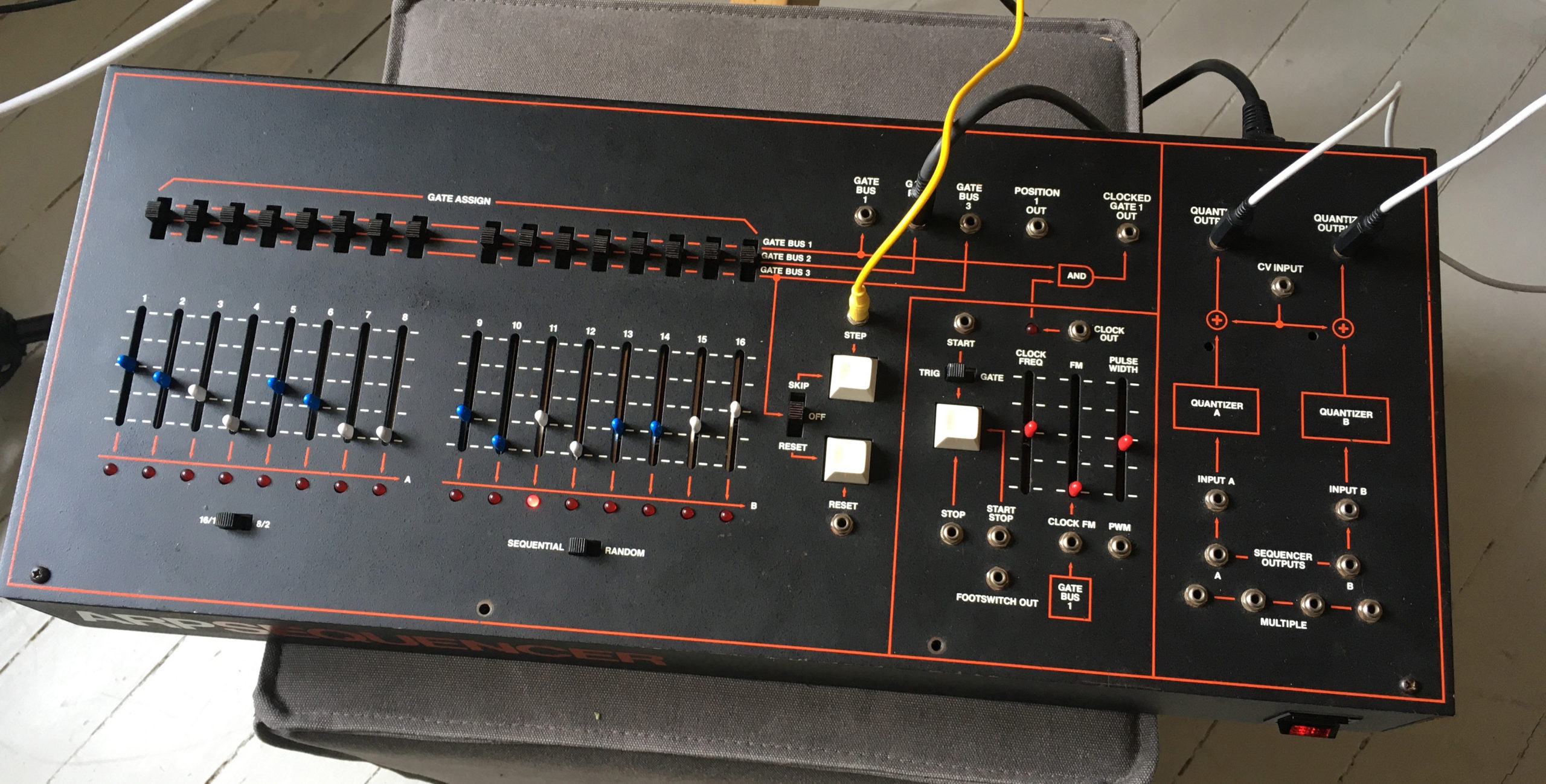
While servicing an Arp Sequencer 1621, I noticed that the three button switches were in a bad shape. One button press would produce anything from one to six signal changes.
These switches can’t be sourced nowadays. The switches are glued together from factory so they can’t be opened.
One possible fix would be to fit some type of modern (long slew) replacement switch inside. You would probably need to design an individual adapter PCB to make it fit the footprint on the 1621 PCB, and also 3D-print an adapter to stick the white button caps back on. However, there’s no guarantee that any other switch will work flawlessly even if it’s new. All electromechanical switches bounce.
I tried removing and washing the switches with ultrasound, warm water and dishwashing detergent. That helped to some extent, but they still exhibited double-triggering and trig on release.

Using the original switches
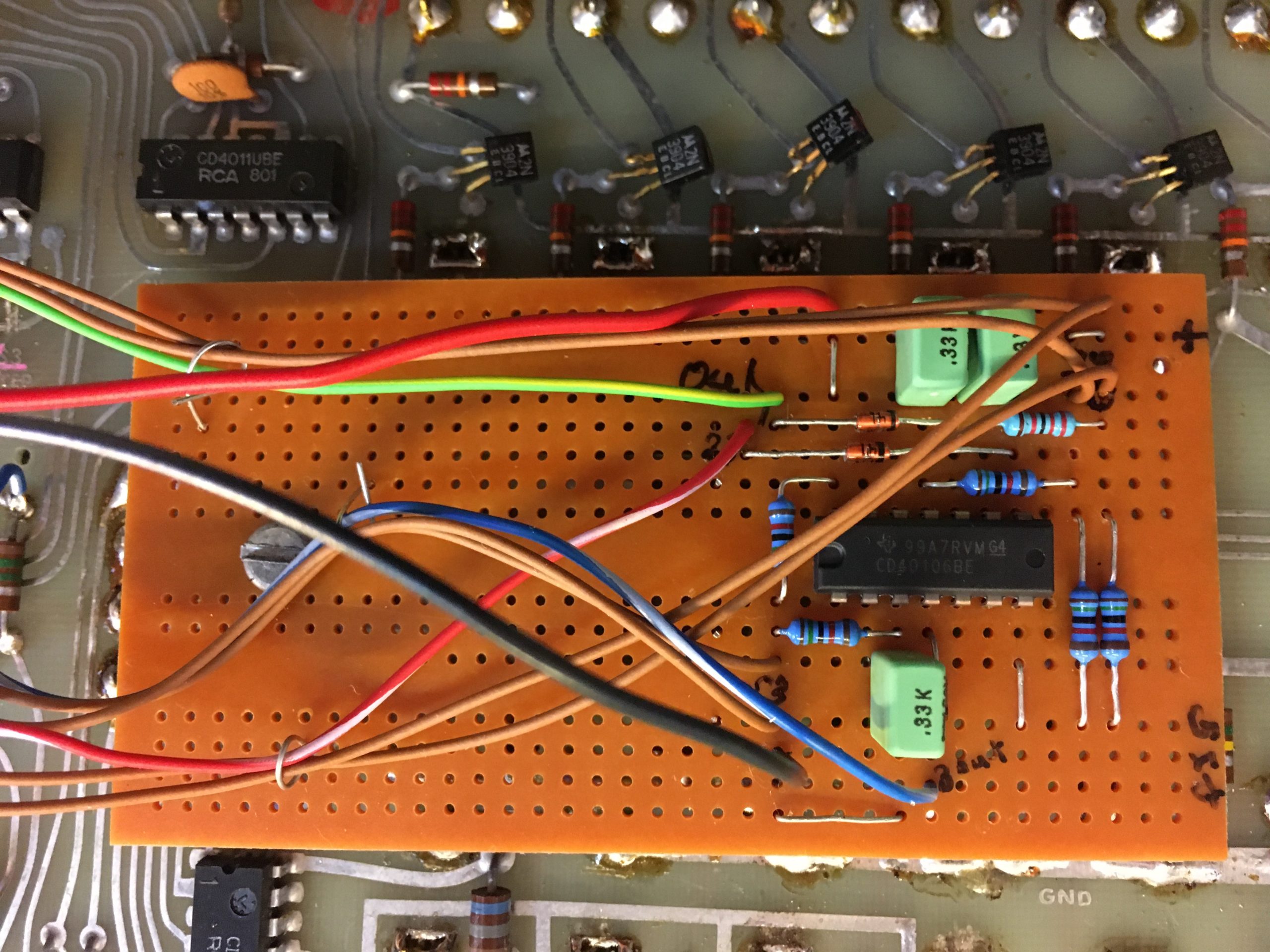
I decided to hardware debounce the switches, using RC filters. I had the following design goals, in addition to making it work:
- Don’t change any components on the 1621 PCB
- Make it visually clear to anyone what my addition does
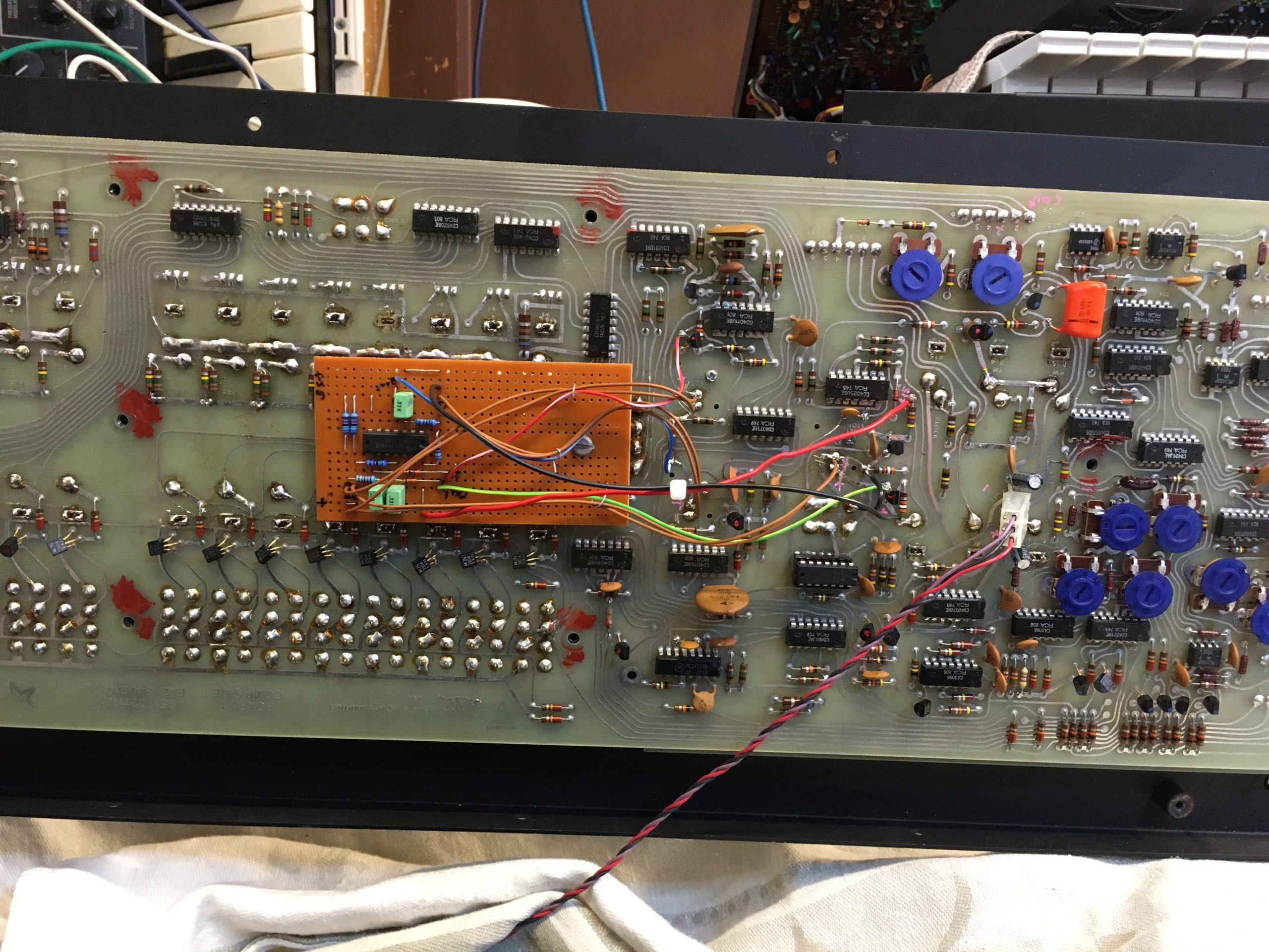
- Stick my PCB to the main PCB, not the bottom of the unit, to keep it simple to open and service
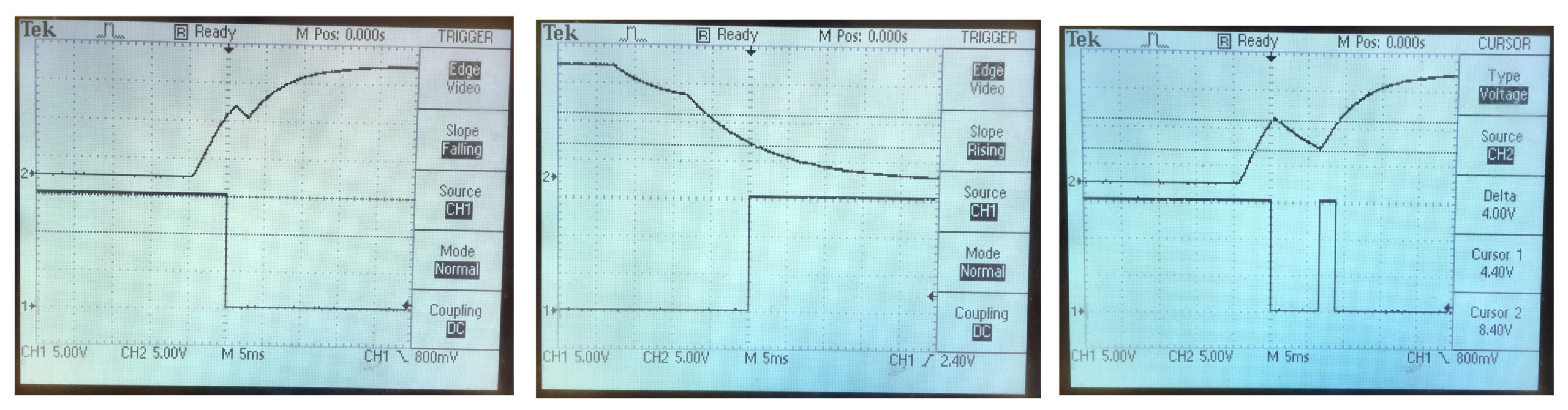
The lower traces in the images above show the RC filtered signal, with the third image showing an extreme case, which I’ve not been able to replicate again. The RC filter will introduce a delay from button press to state change, but it can probably be kept under 10 ms. It depends on how badly degenerated the switches are, their original construction and possibly in what manner they will be hit in actual use: A more firm hit will probably make a shorter period of contact noise (?)
Here some Internet programmer’s well designed RC debounce circuit. Button closing will make pin 1 of U1 see a smooth signal falling towards LOW. Opening the button makes pin 1 see a signal rising to HIGH. The fall and rise rates are defined by R2 * C1 and R1 * C1 respectively.
The diode, while not necessary, makes the charge rate (going towards HIGH) of the capacitor depend only on R1, not R1 + R2.
U1 is an inverter, so the resulting voltage state at pin 2 will be the opposite of pin 1.
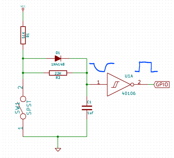
CD40106B inverter
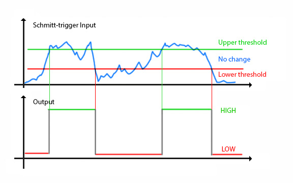
The 40106 is a 20 volt tolerant inverter with Schmitt-trigger. Logic levels in the 1621 are +15 and 0 volt. The Schmitt-trigger handles noise and slowly rising or falling voltages well and is a good companion to the RC filter for debouncing.
There is no technical advantage of inverting the output signal, but the inverter isolates the switch and RC network from from the rest of the circuitry. This can be important when fitting a debounce circuit to an existing system, otherwise you’re likely to unintentionally create voltage dividers that will affect the performance of the debounce circuit, and possibly offset the resulting signal.
Special considerations and adjustments are needed when fitting something like debounce to an existing system. In the 1621 the signals from the switches are later combined with other signals from the input jacks. The original switch construction doesn’t have a HIGH and a LOW state, it has LOW state and UNCONNECTED (in case of the “Start / Stop” and “Reset” switches), and HIGH state and UNCONNECTED (for the Step switch).
Start/Stop Example
When “Start/Stop” switch is UNCONNECTED there’s a weak pull-up that keeps the signal line in HIGH state. This pull-up is weak enough for another connected signal (via External input jack) to pull the line down to LOW if needed.
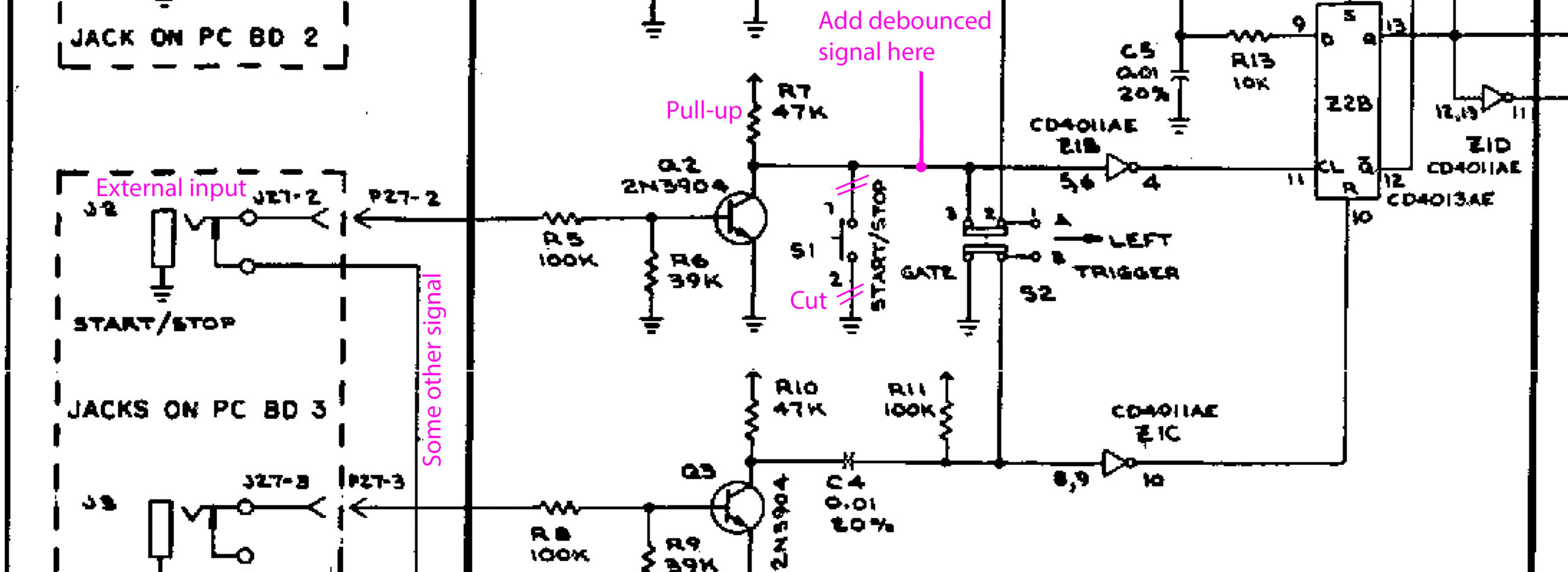
The RC scheme however, can’t have an UNCONNECTED state, only HIGH, LOW or intermediate values. When the debounced switch is off it could therefore affect the “Start/Stop” signal line, and hinder other signals from forcing it LOW. To remedy that, I added D1 and D2 in the following image.
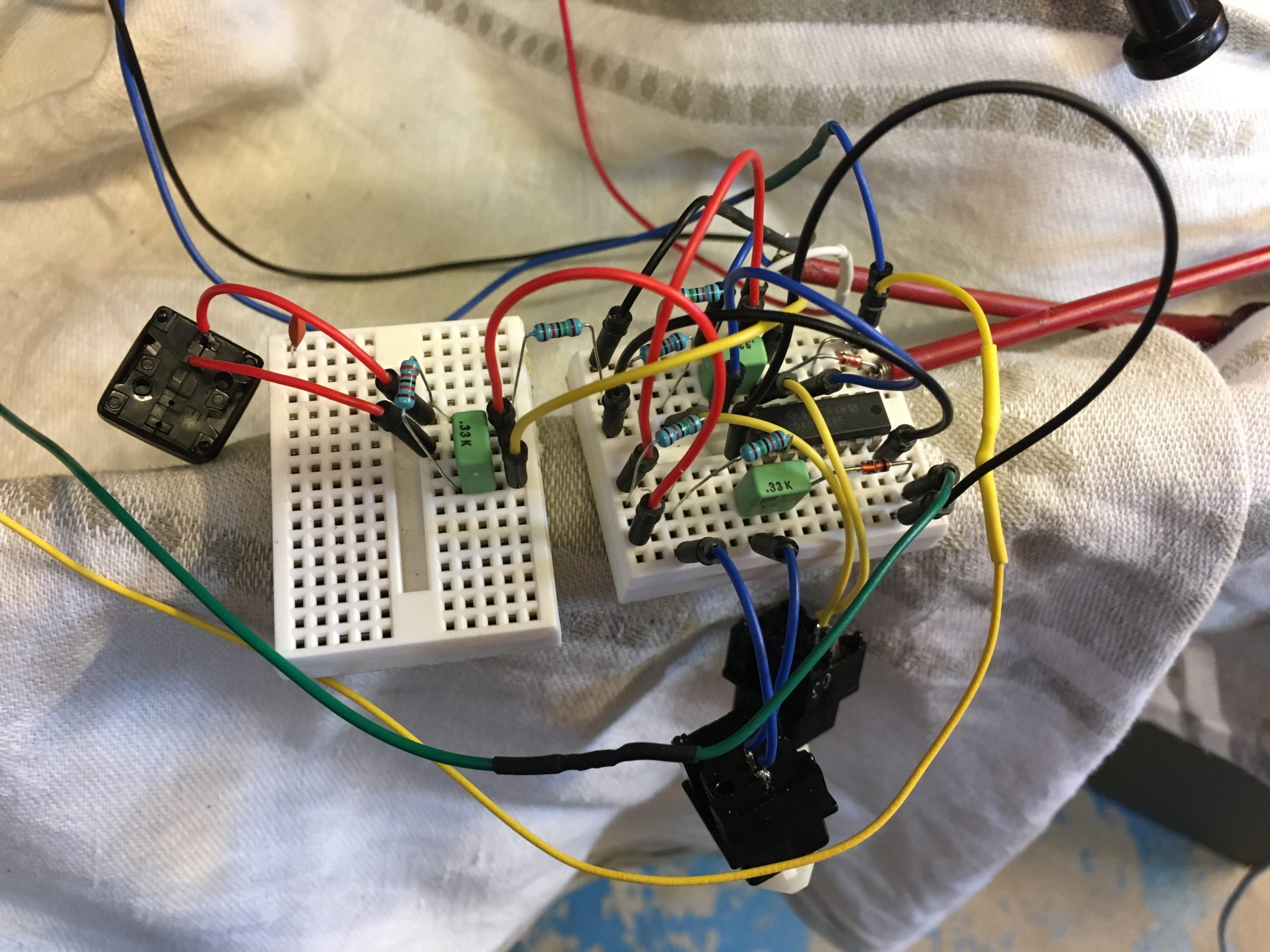
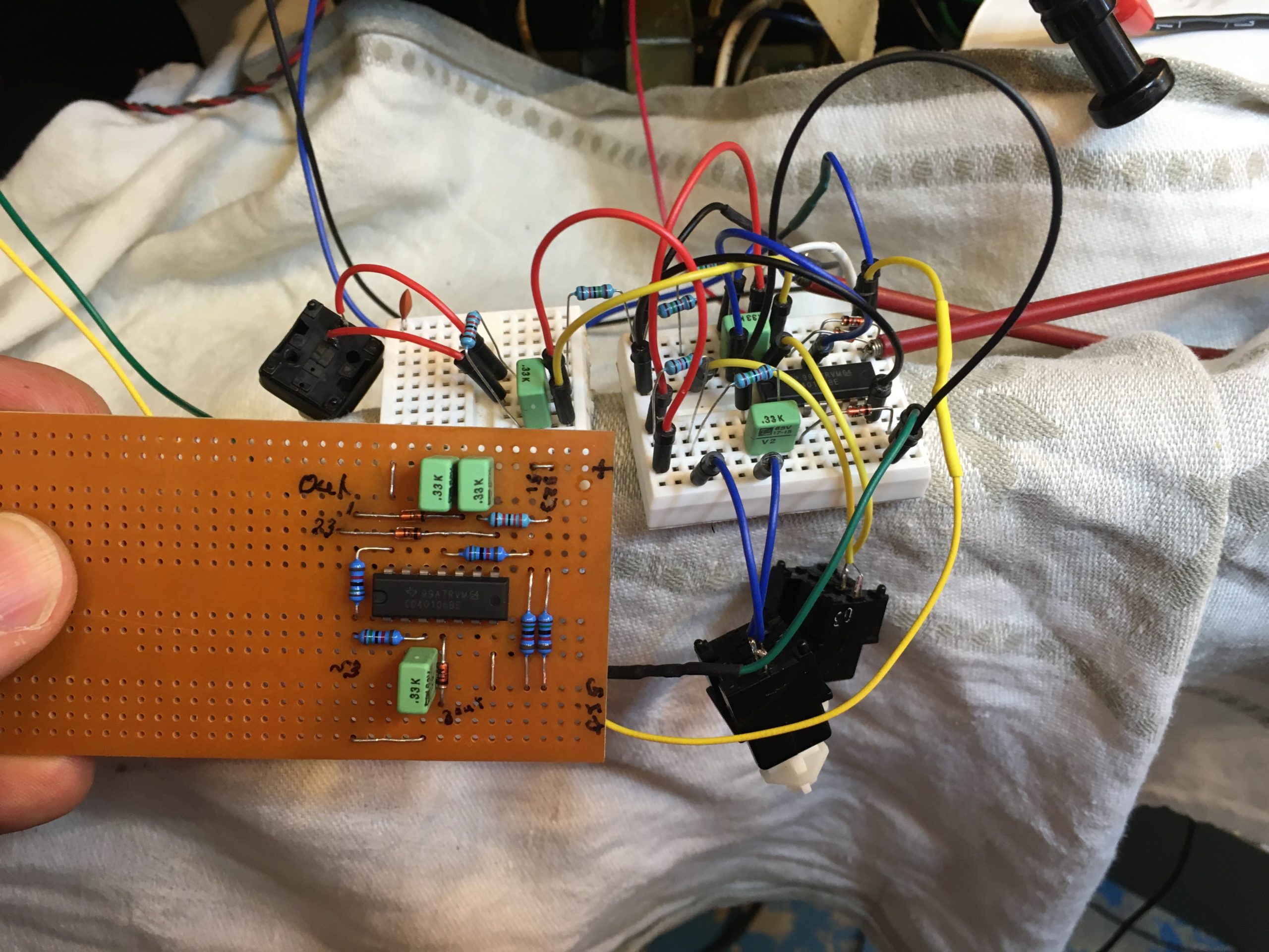
Implementation
The schematic only shows two circuits. That’s because “Reset” and “Start/Stop” use the same top design (except for one resistor value). “Step” uses the bottom design.
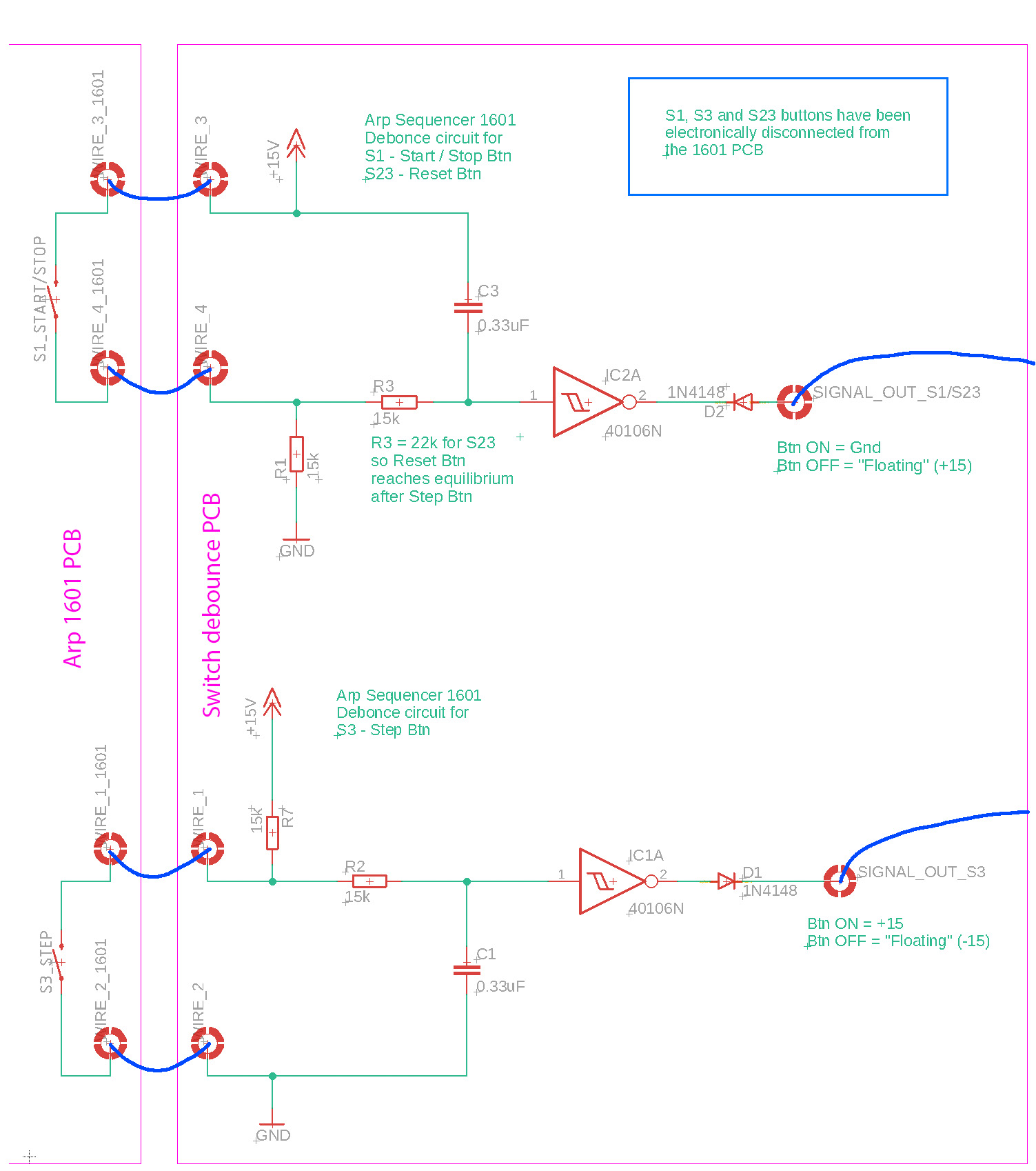
When I tested everything out, I realized that I had created an unwanted behavior in the 1621. Every time I turned the power on, it jumped a number of steps into the sequence, as if the “Step” button had been pressed a few times after startup. That’s natural, since in practice I had delayed the switches by a couple of ms, not only when pressed, but also on startup. I changed R3 to 22k so it would appear to the 1621 as if “Reset” button was pressed a few ms after the other buttons, taking the sequencer back to step 1.

Conclusion
This Arp Sequencer 1621 works as it was intended again. The reaction to button-presses is fast enough, and feels solid and reliable.
I could have done this with a lot fewer wires if I had been more creative with where I cut the PCB paths, in combination with inverting signals once more to get back to uninverted state. But then it would have been much harder to follow the signal flow for the next service technician.
I taped a printout of the schematic, and added a link to this site on the inside of the unit.